- AP plasma roll-to-roll equipment is applied to the surface treatment process for FPCB FCCL PI films
APM – R1600
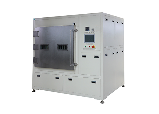
- Vacuum plasma equipment used in PCB decontamination process
Vacuum Plasma Desmear - PVS-DE950
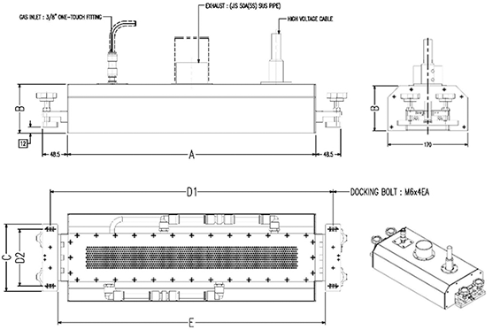
Specification
Electrode quantity
17 EA (Vertical Type)
Number of processed products (FR4)
PCB (550*500 mm2) 16 EA
Equipment
2000×1500×2000 mm3 (W×L×H)
Chamber
1000×1000×950 mm3 (W×L×H)
Power
MF 40 khz, 10 kW
Electrode cooling
Water cooling type
Chiller
5 HP (5 kVA)
Control
PLC control (touch monitor)
MFC
O2, CF4, N2, Ar
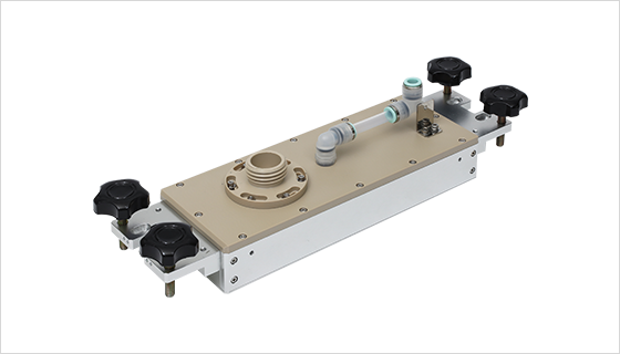
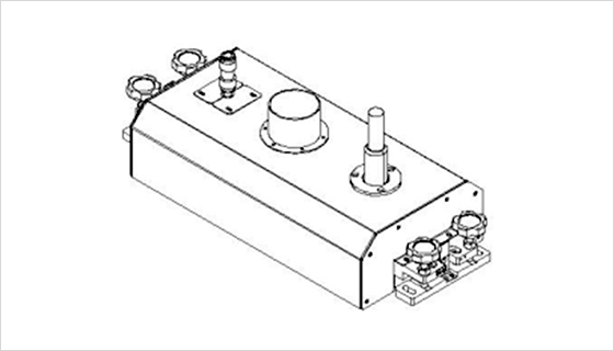
Vacuum Plasma Desmear
1. Uniform removal of epoxy residues (smear) generated during the PCB drilling process / Securing product reliability
2. It consumes a small amount of gas, and has a low running cost due to no chemical disposal cost
3. Various plasma treatment processes are possible, which enables hydrophilic surface modification, and reduction process, so on in addition to de-smearing.